
Made a FSAE Electric accumulator safety light indicating when
high voltage is present, utilizing a 60-450V Flyback Converter
ROLE
SUMMARY
DURATION
HV Lead — Team Phantom SFU FSAE Electric
Jul 2024 - Feb 2026
ACCUMALTOR INDICATOR LIGHT
ACCUMALTOR INDICATOR LIGHT
ACCUMULATOR INDICATOR LIGHT
High Voltage PCB Design
Schematic Capture
Trouble Shooting
High Voltage Testing
LTspice
Power Electronics
Analog Electronics
OVERVIEW
Formula SAE Electric requires a bright red safety light on the accumulator to indicate when high voltage (HV) is present, defined as a system voltage above 60V. I designed a custom 60–450V flyback converter to power the indicator light and reliably activate it at 57V, providing a clear indication before the accumulator reaches the 60V HV threshold.
CONSTRAINTS / REQUIREMENTS
There are a couple difficulties associated with this project that guided it's design:
Not being able to use any other low voltage sources (5V, 12V, etc.) in the car for the full 0-400V system voltage range
Designing around high voltage and utilizing galvanic isolation
Finding a converter that could handle the unusually wide input voltage range (0-400V), for which no compact, off-the-shelf converters exist at a reasonable cost
DESIGN
3.1 CONCEPTUAL
What is a flyback converter? A flyback is a buck-boost converter that outputs a fixed voltage for input voltages greater than OR less than the output voltage.
The flyback converter should be understood by what happens when the NMOS is switched ON and OFF.
When the NMOS is ON, the primary side coil of the transformer is grounded and energy is stored in the primary coil in the form of magnetizing inductance. At the same time current is prevented to flow on the secondary and tertiary side by diodes and the reverse polarity coil winding.
When the NMOS is OFF, the magnetizing inductance in the primary discharges it's stored energy/current into the secondary and tertiary with some coil ratio which provides our power for the output.
Another explanation by Digikey: here
We then use feedback to measure the level of the output voltage and switch the converter quickly, 17.8kHz in my setup, to maintain the desired output voltage.

3.2 SCHEMATIC DETAILS
Specific design details:
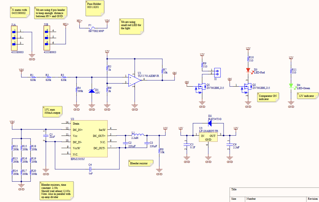
A diode–zener snubber across the primary winding of the transformer clamps and discharges voltage spikes and excess energy caused by leakage inductance when the NMOS switches OFF, preventing potentially destructive overvoltage on the NMOS.
The NMOS gate is driven by a Pulse-Frequency Modulation (PFM) signal from the controller IC. Switching frequency varies with output load and voltage operating at 17.8 kHz for the selected indicator light.
A voltage divider sets the controller's enable threshold, turning on the converter and thus the indicator light when the HV input reaches 57V.
The controller compensates for changes in the secondary-side diode forward voltage drop due to temperature rise, which is important since it's used to set output voltage and without it output voltage may stray overtime. Wider PCB copper pours are used in board design to dissipate heat better and minimize temperature change.
A voltage divider provides feedback from the transformer tertiary winding, regulating the output to approximately 15.8V.
A shunt resistor senses primary-side current and sets the maximum output current to 1A in my configuration. This can be adjusted should we require it.
A cartridge fuse is used on the up to 400V input, sized for 600VDC, 5A current rating and 10kA interrupt rating.
Output filter capacitors reduce voltage ripple using a bulk capacitor supplemented by parallel bypass capacitors to reduce effective ESR.
A linear regulator steps the filtered 15.8V output down to 12V for the indicator light, providing a clean supply and minimizing the impact of residual switching ripple
3.3 PCB Design
Specific design details:
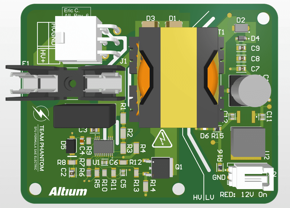
Wide copper pours are used for high current paths
Thermal vias are used on flyback IC and regulator GND connections
400V and HVGND come onto the board on opposite pins of the header to maintain greater than 3mm clearance according to IEC 60664-1
Greater than 8mm creepage is maintained between HV and LV, with slots implemented for close quarters according to IEC 60664-1
HVGND and LVGND planes are on the bottom layer and are also separated with 8mm creepage in the case of a HV fault and HVGND becomes HV
Probe touch points are used for important signals for debugging
An SMD indicator LED is used on output for debugging
3.3 TESTING
Made a test plan to test the board
Tested the board with up to 400V
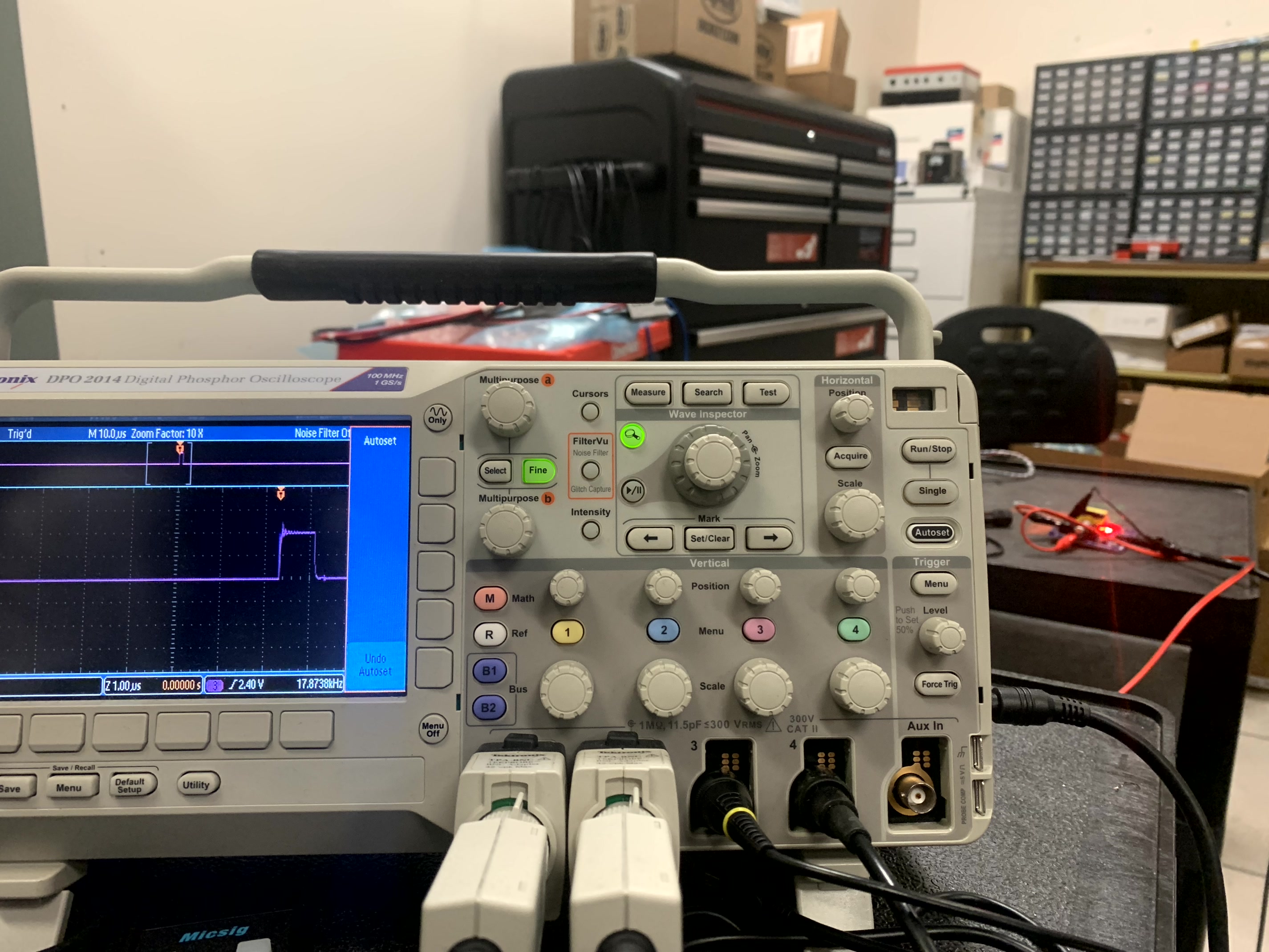
Light turned on at around 57.2V
Saw 12V on the output for the entire 57-400V test range using the probing points
Approx. PFM Frequencies for different input voltages on the switching MOSFET:
57V: 6.2kHz
200V: 18.7kHz
300V: 17.8kHz
400V: 17.2kHz


ITERATIONS
4.1 ITERATION 1
The first revision of the board I worked on and my first time designing a schematic and PCB, evidently
Board concept was to step down HV with a regulator to use as a reference for a comparator and use a voltage divider on HV for comparator to switch a NMOS for powering a light once 60V was reached. It also powered the light by limiting current with a resistor grid and a zener to clamp voltage
Main problems with this board:
The regulator is not rated to withstand 400V
The zener was not rated to clamp 400V to 20V, even if you limit the current for power dissipation
The MOSFET was the wrong way lol
This was not manufactured, thankfully


4.2 ITERATION 2
This iteration does the same sort of thing as the last but uses 2 linear regulators in parallel for powering the LED
Main problems:
This is still not valid because regulators are not rated to withstand 400V
It is not initially clear how two regulators in parallel would behave, as they might begin to fight each other to regulate the same output voltage or one of the regulators might just not work while the other provides all the current. Either way I designed this originally with a complete lack of understanding of proper regulator implementation so, but it is still interesting thought expirement.
I used a voltage divider on output of the regulators with the intention of stepping down the voltage into the NMOS but this is incorrect as the node is not high impedance and the current draw would just break the divider rendering it into a pull-down and more current limiting on my LED.
Some other funny things is R9 on a high impedance input and R8 limiting current for the comparator VCC which would at-best cause it to likely turn off when output is high due to lack of power and at worst cause it to not turn on at all.
Still learned about fusing and starting to take into consideration voltage limits for component selection


4.3 ITERATION 3
Learned my lesson this time by using an isolated converter module that could handle 400V instead of regulators
Pretty simple converter implementation so nothing very wrong except using a resistor grid to spread power which is a little weird when you can just get a single resistor with a higher power rating but I think I was too stubborn to use any size other than 0805 or get something more expensive than standard resistor price
Ended up assembling and testing this
Funny thing with the board design was that there wasn't a footprint for the converter in Altium so I ended up making it from the datasheet but I didn't realize it was the bottom view so when I assembled the board, the converter was on the other side


Tested with 400V
The board worked but technically this wasn't rules legal because it would turn on the light at whatever it's minimum input voltage was, not 60V
We initially thought it would be fine since realistically our system voltage could not go below about 300V because then we would be undercharging our 18650 cells and damaging them, but we decided to make another revision
Another problem with this design that we realized after testing is that there were no bleeder resistors for the 22uF cap of the converter so once we tested the board, it just had 400V of charge sitting on it waiting to give someone a nasty shock, and the converter didn't want to discharge it, so we air-discharged it over a couple days

4.4 ITERATION 4
This board uses a similar strategy as the previous board where it uses a converter to step down voltage for powering the light and for using as a reference for a comparator to switch a NMOS
The converter has a range of 110-450V but I saw in the datasheet an input derating curve (here, page 3) that said I could use the converter down to 50V, just at a fraction of the max load current, so I thought I could getaway with using the same converter since my current draw wasn't near the max
I could not :(
Tested it and it only turned on at 110V
Some other board improvements/issues:
I completely break the isolation that the converter gives me here and the comparator is not setup for isolation
The bleeder resistor grid can again likely be setup with a single resistor with a higher power rating and size or maybe 2, max 3, resistors in series with your desired equivalent resistance if your worried about creepage between resistor pads
It would have been better practice to add a bypass on the comparator VCC and a gate resistor on the comparator output for mosfets

4.5 FINAL ITERATION
Current design
Solves problems of previous converters by having wide enough input voltage range to handle the full 0-400V range
Actually implements creepage, clearance and other HV design practices

